Table of Contents
DL10J
RS232/422/485 Assignment
| RS-232 | RS-422 | RS-485 | ||
|---|---|---|---|---|
 | PIN | COM | COM | COM |
| 1 | DCD1# | 422 TX - | 485 - | |
| 2 | SIN1 | 422 TX + | 485 + | |
| 3 | SOUT1 | 422 RX - | ||
| 4 | DTR1 | 422 RX + | ||
| 5 | GND | |||
| 6 | DSR1# | |||
| 7 | RTS1 | |||
| 8 | CTS1# | |||
| 9 | RI1# |
Software Installation and First Connect WWN01 LTE Module + Huawei EM906S LTE Module
 Please note: Before performing the below steps, please install the hardware according to the installation guide as found in the specification PDF.
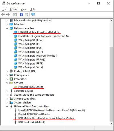
- Please run Windows Update in order to install the driver for the HUAWEI GNSS Sensor. The other two components will use the Windows 10 inbox driver (1803 and newer).
- Once the Windows Update process is completed, three devices should be listed in the device manager as shown below.
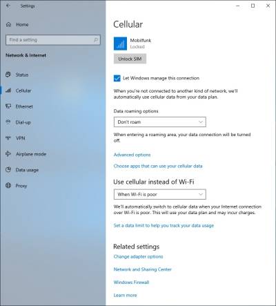
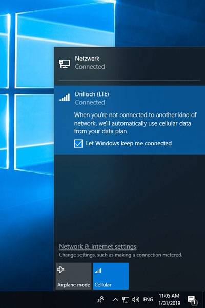
- Check Windows Settings in Network & Internet for the newly available Cellular connection.
- Here, you can also select under which conditions the Cellular connection should be used.
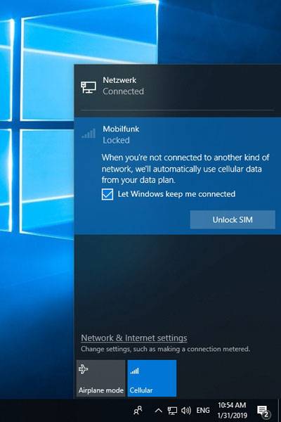
- The Cellular connection is also visible in the Network Tray Symbol, just where usually Wi-Fi signals can be found.

Click “Unlock SIM” to connect.
- Enter the PIN (if applicable) of your SIM card and press “Next”.
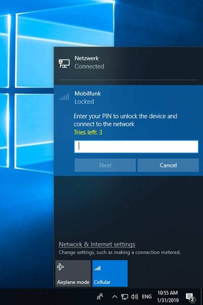
- If the PIN was entered correctly and the SIM card is enabled for DATA connection, the connection should now be set up.
Which LTE/4G modules are suitable?
Successfully tested M.2-3042 modules:
| Brand | Model | |
|---|---|---|
| Sierra | EM7455 | CAT 6, for Europa and North America |
| Sierra | EM7430 | CAT 6, for APAC |
| Huawei | ME906S | CAT 4, for EMEA, Australia, New Zealand |
| Quectel | EM06-E | CAT 6, for EMEA, Australia, Brazil |
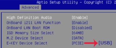
LTE module cannot be found in the device manager?
Check the following BIOS setting to ensure that the LTE module will be recognized correctly.
Go to Advanced → Onboard Device Configuration → E → Key Device Select and change from PCIE to USB
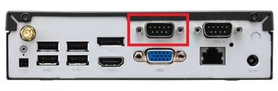
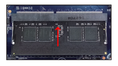
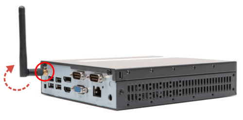
Where is COM port #1?
The first COM port is marked on this photo:
Quick Installation Guide
Begin Installation
For safety reasons, please ensure that the power cord is disconnected before opening the case.
- Unscrew the two screws of the chassis cover.
- Slide the cover backward and upward.
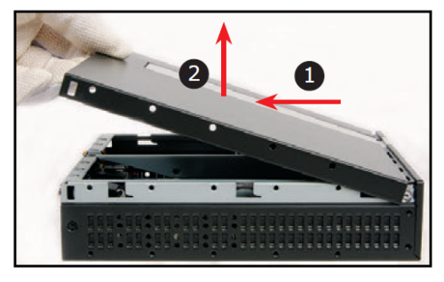
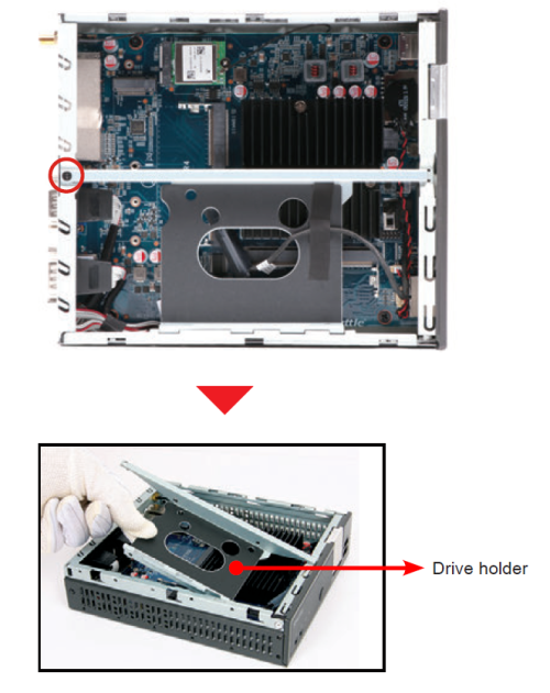
- Unfasten the rack mount screw and remove the drive holder.
Memory Module Installation
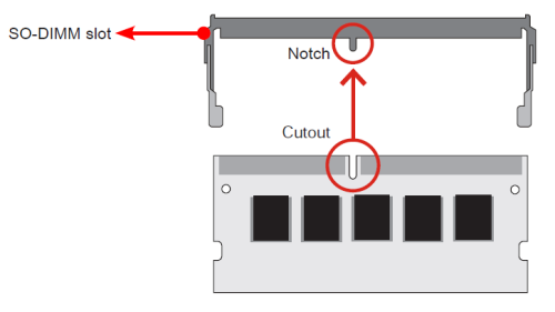
This mainboard does only support 1.2 V DDR4 SO-DIMM memory modules.
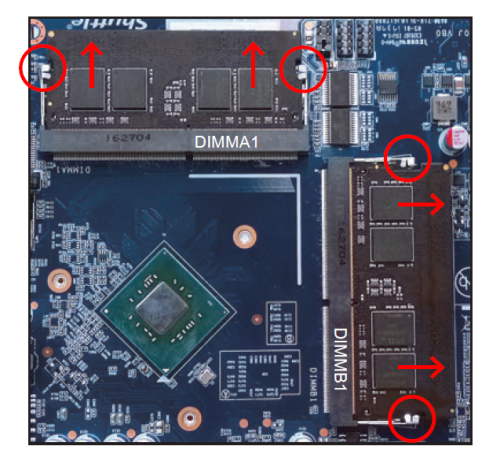
- Locate the SO-DIMM slot on the mainboard.
- Align the notch of the memory module with the one of the relevant memory slot.
- Gently insert the module into the slot in a 45-degree angle.
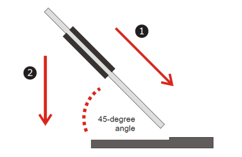
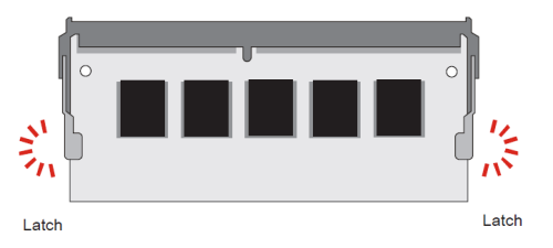
- Carefully push down the memory module until it snaps into the locking mechanism.
- Repeat the above steps to install an additional memory module, if required.
Component Installation
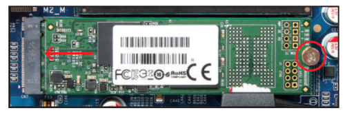
- Please proceed as shown in the illustration, and locate the M.2 key slot on the mainboard.
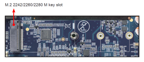
- Install the M.2 device in the M.2 slot and secure with the screw.
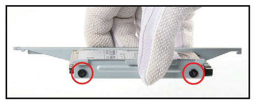
- Place an HDD or SSD in the rack and secure with four screws from the sides.
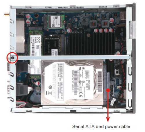
- Connect the Serial ATA and power cable to the HDD or SSD. Slide the rack into the chassis and refasten the screws.
Complete
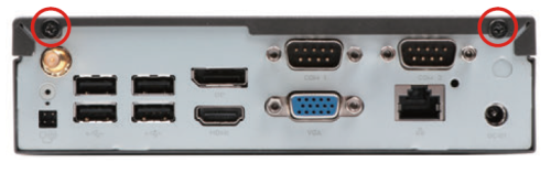
- Replace the cover and refasten the screws.
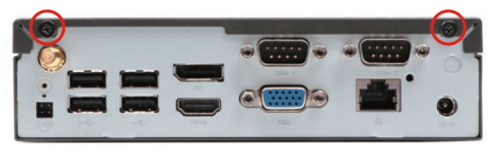
- Screw the included antenna on to the appropriate connector at the back panel. Make sure it is aligned vertically or horizontally to achieve the best possible signal reception.
- Complete.
- Please press the
Delkey while booting to enter BIOS. Here, please load the optimised BIOS settings.
Jumper settings and pinout
SATA cable connector (SATA1)
1=NA
2=NA
3=NA
4=NA
5=GND
6=GND
7=GND
8=+5V
9=+5V
10=+5V
11=+5V
12=GND
13=GND
14=GND
15=SATA_TX_P
16=SATA_TX_N
17=GND
18=SATA_RX_N
19=SATA_RX_P
20=GND
AC back auto power on (JP1)
1=OP(+)
2=GND
Clear CMOS & power button (SW1)
1=RTCRST
2=+5V
3=GND
4=PWRSW
Battery connector (CN9)
1=V_BAT
2=GND
Debug port (DBG1)
1=LPC_24M
2=LAD1
3=SIORST-
4=LAD0
5=LFRAME-
6=+3.3V
7=LAD3
8=GND
9=LAD2
10=NULL
COM 1 & COM 2 power switch (JP2)
COM PORT Pin 9 “Ring Indicator” (RI) configuration:
Configure COM 1 with the first jumper:
- Short Pin 1-2: Pin 9 = RI (default)
- Short Pin 5-7: Pin 9 = +5V
- Short Pin 7-9: Pin 9 = +12V
Configure COM 2 with the second jumper:
- Short Pin 3-4: Pin 9 = RI (default)
- Short Pin 6-8: Pin 9 = +5V
- Short Pin 8-10: Pin 9 = +12V
1=-XRI1
2=COM_-XRI1
3=-XRI2
4=COM_-XRI2
5=+5V
6=+5V
7=COM1_PWR
8=COM2_PWR
9=+12V
10=+12V
COM port (COM 1, COM 2)
1=DCD
2=RX
3=TX
4=DTR
5=GND
6=DSR
7=RTS
8=CTS
9=RI
10=NULL